Electric Magnetic Field Mapping

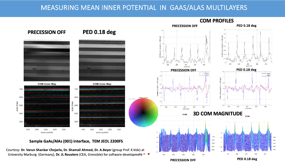
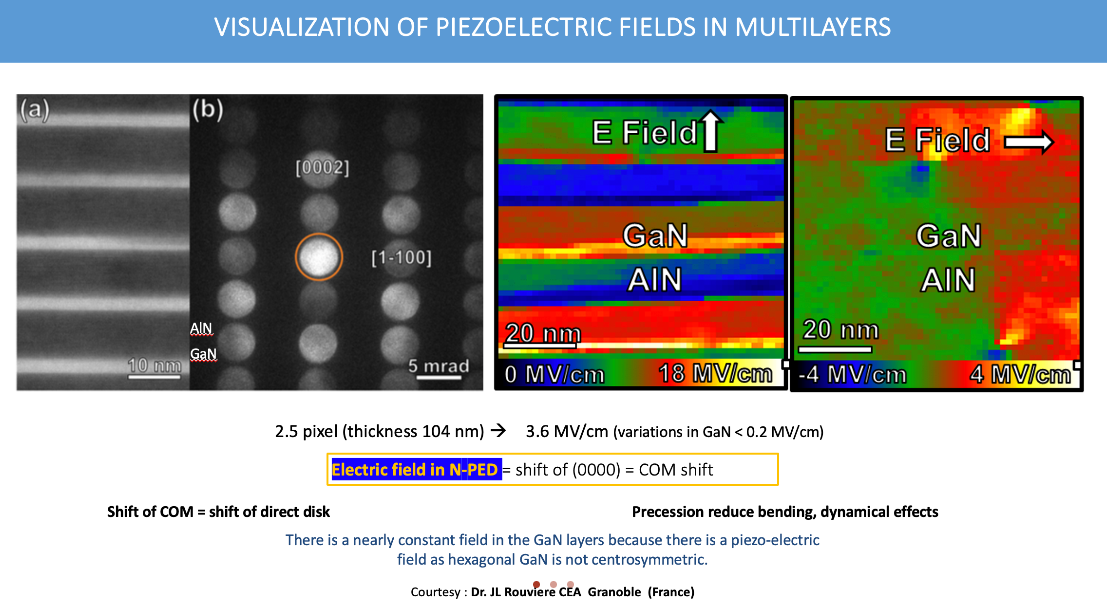
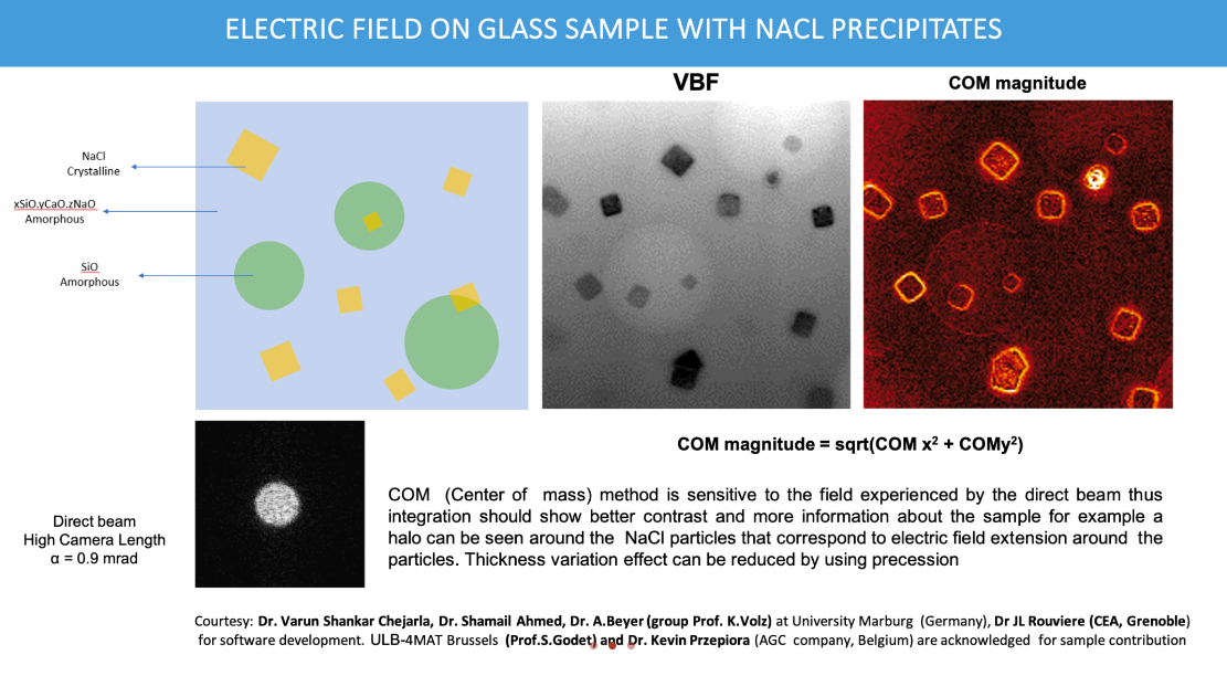
4D-Scanning Precession Electron Diffraction (4D-SPED) in TEM is an advanced technique for high-resolution materials characterization, enabling precise orientation, phase, and strain mapping. By scanning the electron beam and capturing diffraction patterns at each point, it reveals local electric and magnetic fields. Enhanced by controlled beam precession, it delivers accurate, low-noise data for analyzing modern materials and nanoscale devices.

APPLICATION NOTE

Design Materials with Specific Applications

Challeging Materials with Challenging Applications

Better Steel with Improved Properties

Steel Corrosion in Nuclear Plants

Metals Under Huge Stress

Pavements of the Nanoworld

Structure of Embedded Nanodomains

Nanoscale Reaction Models in Solid Oxide Fuel Cells

Inside the Structure of Dye-Sensitized Solar Cells

Understanding Li insertion for next generation batteries

From “Clean Energy” Cars to Structure of Metal Organics MOFs

Next generation circuits for semiconductor industry

Structure of magnetic semiconductors

Atomic scale of nanolayer composites

Architecture of hybrid nanocrystalline microporous materials

Structure of new Sarrabusite mineral

Structure of intriguing meso-micrporous zeolites

Drug delivery & Structure of Nanoparticles

Inside the nanowire forest