Auto Strain Mapping

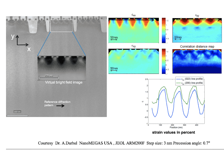
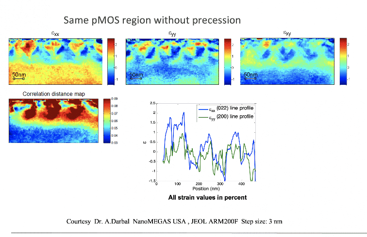
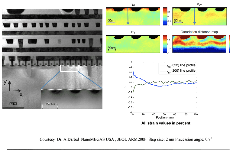
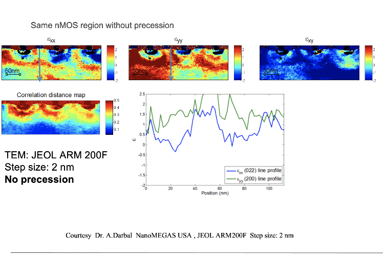
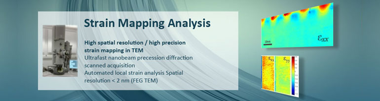
Novel Automated Strain Mapping Solution for TEM/STEM (Patent pending) based on nanobeam precession diffraction patterrns in combination with DigiSTAR. Precision up 0.02% (200kV FEG) with spatial resolution up to 2nm attainable (FEG-TEM). Measurement of strain with high spatial resolution and high precision in semiconductor devices is critical to monitor the designed and unintended strain distributions.

Auto Strain Mapping Specification

APPLICATION NOTE

Design Materials with Specific Applications

Challeging Materials with Challenging Applications

Better Steel with Improved Properties

Steel Corrosion in Nuclear Plants

Metals Under Huge Stress

Pavements of the Nanoworld

Structure of Embedded Nanodomains

Nanoscale Reaction Models in Solid Oxide Fuel Cells

Inside the Structure of Dye-Sensitized Solar Cells

Understanding Li insertion for next generation batteries

From “Clean Energy” Cars to Structure of Metal Organics MOFs

Next generation circuits for semiconductor industry

Structure of magnetic semiconductors

Atomic scale of nanolayer composites